
The first transistor: date and history of invention, principle of operation, purpose and application
Who created the first transistor? This question worries a lot of people. The first patent for the field effect transistor principle was filed in Canada by the Austro-Hungarian physicist Julius Edgar Lilienfeld on October 22, 1925, but Lilienfeld did not publish any scientific papers on his devices and his work was ignored by the industry. Thus, the world's first transistor has sunk into history. In 1934, German physicist Dr. Oskar Heil patented another FET. There is no direct evidence that these devices were built, but later work in the 1990s showed that one of Lilienfeld's designs worked as described and yielded a substantial result. It is now a known and generally accepted fact that William Shockley and his assistant Gerald Pearson created working versions of the apparatus from Lilienfeld's patents, which, of course, was never mentioned in any of their later scientific works or historical articles. The first computers based on transistors, of course, were built much later.
Bell Lab
Bell Labs worked on a transistor built to produce extremely pure germanium "crystal" mixer diodes used in radar installations as part of the frequency mixer. Parallel to this project, there were many others, including the germanium diode transistor. Early tube-based circuits did not have fast switching capability, and the Bell team used solid-state diodes instead. The first transistorized computers worked on a similar principle.
Further exploration of Shockley
After the war, Shockley decided to try to build a triode-like semiconductor device. He secured funding and lab space, and then worked on the problem with Bardeen and Bratten. John Bardeen eventually developed a new branch of quantum mechanics known as surface physics to explain his early failures, and these scientists eventually succeeded in creating a working device.
The key to the development of the transistor was the further understanding of the process of electron mobility in a semiconductor. It was proven that if there was some way to control the flow of electrons from emitter to collector of this newly discovered diode (discovered 1874, patented 1906), an amplifier could be built. For example, if you place contacts on either side of one type of crystal, no current will flow through it.
In fact, it turned out to be very difficult to do this. The crystal size would have to be more average, and the number of supposed electrons (or holes) that needed to be "injected" would be very large, which would make it less useful than an amplifier because it would require a large injection current. However, the whole idea of the crystal diode was that the crystal itself could hold electrons at a very short distance, while being almost on the verge of depletion. Apparently the key was to keep the input and output pins very close to each other on the crystal surface.
Proceedings of Bratten
Bratten began working on such a device, and hints of success continued to surface as the team worked on the problem. Invention is hard work. Sometimes the system works, but then another failure occurs. Sometimes the results of Bratten's work began to work unexpectedly in water, apparently due to its high conductivity. Electrons in any part of the crystal migrate due to nearby charges. The electrons in the emitters or "holes" in the collectors accumulated directly on top of the crystal, where they receive the opposite charge, "floating" in the air (or water). However, they could be pushed off the surface by applying a small amount of charge from anywhere else on the crystal. Instead of requiring a large supply of injected electrons, a very small number in the right place on the chip will do the same thing.
The new experience of the researchers to some extent helped to solve the previously encountered problem of a small control area. Instead of having to use two separate semiconductors connected by a common but tiny area, one large surface will be used. The emitter and collector outputs would be at the top, and the control wire would be placed at the base of the crystal. When a current was applied to the "base" terminal, the electrons would be pushed through the semiconductor block and collected on the far surface. As long as the emitter and collector were very close together, this would have to provide enough electrons or holes between them to start conduction.
Accession of Bray
An early witness to this phenomenon was Ralph Bray, a young graduate student. He joined the development of the germanium transistor at Purdue University in November 1943 and was given the difficult task of measuring the leakage resistance of a metal-semiconductor contact. Bray found many anomalies, such as internal high-resistance barriers in some germanium samples. The most curious phenomenon was the exceptionally low resistance observed when voltage pulses were applied. The first Soviet transistors were developed on the basis of these American developments.
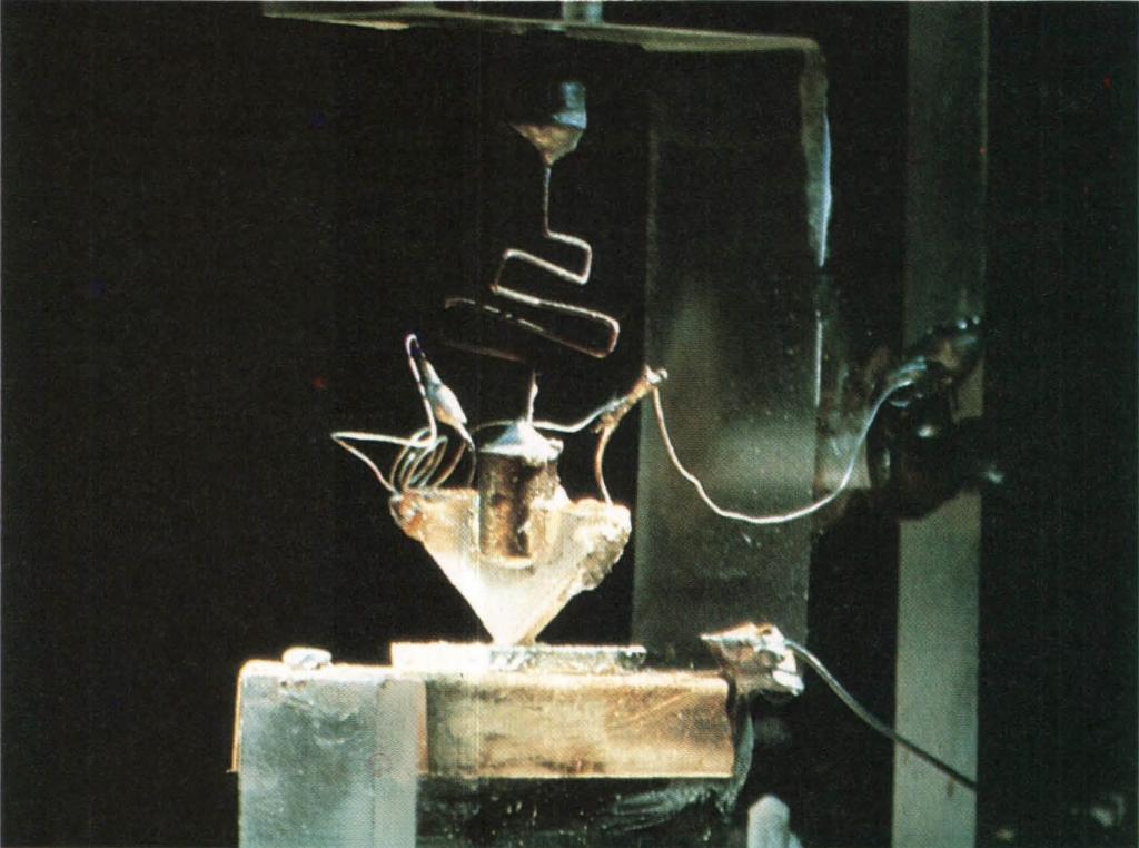
Breakthrough
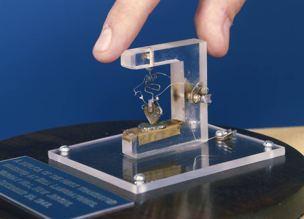
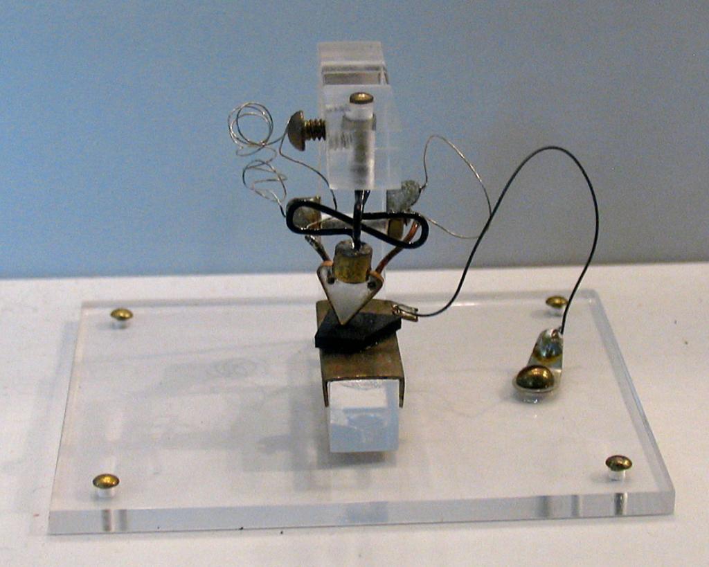
On December 16, 1947, using a two-point contact, contact was made with a germanium surface anodized to ninety volts, the electrolyte was washed into H 2 O, and then several gold spots fell on it. Gold contacts were pressed against bare surfaces. The separation between the dots was about 4×10 -3 cm. One dot was used as a grid and the other dot as a plate. The deviation (DC) on the grid had to be positive to get a voltage power gain at the plate bias of about fifteen volts.
Invention of the first transistor
Many questions are connected with the history of this miracle mechanism. Some of them are familiar to the reader. For example: why were the first transistors of the USSR PNP-type? The answer to this question lies in the continuation of this whole story. Bratten and H. R. Moore demonstrated to several colleagues and managers at Bell Labs on the afternoon of December 23, 1947, the result they had achieved, which is why this day is often cited as the birth date of the transistor. A PNP-contact germanium transistor worked as a speech amplifier with a power gain of 18. This is the answer to the question why the first transistors of the USSR were PNP-type, because they were purchased from the Americans. In 1956, John Bardeen, Walter Houser Bratten and William Bradford Shockley were awarded the Nobel Prize in Physics for their research on semiconductors and the discovery of the transistor effect.
Twelve people are mentioned as being directly involved in the invention of the transistor at Bell Laboratories.
The very first transistors in Europe
At the same time, some European scientists got excited about the idea of solid-state amplifiers. In August 1948, German physicists Herbert F. Matare and Heinrich Welker, working at the Compagnie des Freins et Signaux Westinghouse in Aulnay-sous-Bois, France, applied for a patent for an amplifier based on a minority of which they called "transistor". Because Bell Labs did not publish the transistor until June 1948, the transistor was considered independently developed. Mataré first observed the effects of transconductance in the production of silicon diodes for German radar equipment during World War II. Transistors were commercially made for the French telephone company and the military, and in 1953 a four-transistor solid state radio was demonstrated at a radio station in Düsseldorf.
Bell Telephone Laboratories needed a name for a new invention: Semiconductor Triode, Tried States Triode, Crystal Triode, Solid Triode, and Iotatron were all considered, but John R. Pierce's "transistor" was the clear winner of an internal vote (due in part to the closeness the engineers Bell was developed for the suffix "-istor").
The world's first commercial transistor production line was at the Western Electric plant on Union Boulevard in Allentown, Pennsylvania. Production began on October 1, 1951 with a point contact germanium transistor.
Further application
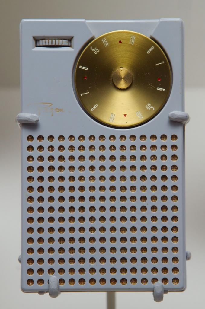
Up until the early 1950s, this transistor was used in all kinds of manufacturing, but there were still significant problems preventing its wider use, such as sensitivity to moisture and the fragility of wires attached to germanium crystals.
Shockley was often accused of plagiarism due to the fact that his work was very close to the work of the great but unrecognized Hungarian engineer. But Bell Labs attorneys quickly settled the issue.
Nevertheless, Shockley was outraged by the attacks from critics and decided to demonstrate who was the real brain of the whole great epic of the invention of the transistor. Just a few months later, he invented a completely new type of transistor with a very peculiar "sandwich structure". This new form was much more reliable than the fragile point-contact system, and it was this form that ended up being used in all transistors of the 1960s. It soon developed into the bipolar junction apparatus, which became the basis for the first bipolar transistor.
The static induction device, the first concept of a high-frequency transistor, was invented by Japanese engineers Jun-ichi Nishizawa and Y. Watanabe in 1950 and was finally able to create experimental prototypes in 1975. It was the fastest transistor in the 80s of the twentieth century.
Further developments included extended junction, surface barrier, diffusion, tetrode, and pentode transistors. The diffusion silicon "mesa transistor" was developed in 1955 at Bell and commercially available from Fairchild Semiconductor in 1958. The space was a type of transistor developed in the 1950s as an improvement over the point contact transistor and the later alloy transistor.
In 1953, Filco developed the world's first high-frequency surface barrier device, which was also the first transistor suitable for high-speed computers. The world's first transistorized car radio, made by Philco in 1955, used surface barrier transistors in its circuitry.
Problem solving and improvement
With the solution of the problems of fragility, the problem of cleanliness remained. Producing germanium of the required purity proved to be a major challenge and limited the number of transistors that could actually work from a given batch of material. The temperature sensitivity of germanium also limited its usefulness.
Scientists have speculated that silicon would be easier to manufacture, but few have explored this possibility. Morris Tanenbaum at Bell Laboratories were the first to develop a working silicon transistor on January 26, 1954. A few months later, Gordon Teal, working on his own at Texas Instruments, developed a similar device. Both of these devices were made by controlling the doping of single silicon crystals as they were grown from molten silicon. A higher method was developed by Morris Tanenbaum and Calvin S. Fuller at Bell Laboratories in early 1955 by gaseous diffusion of donor and acceptor impurities into single crystal silicon crystals.
FETs
The FET was first patented by Julis Edgar Lilienfeld in 1926 and Oskar Hale in 1934, but practical semiconductor devices (transition field effect transistors) were developed later, after the effect of the transistor was observed and explained by William Shockley's team at Bell Labs in 1947 immediately after the expiration of the twenty-year patent period.
The first type of JFET was the static induction transistor (SIT) invented by Japanese engineers Jun-ichi Nishizawa and Y. Watanabe in 1950. SIT is a type of JFET with a short channel length. The metal-oxide-semiconductor semiconductor field-effect transistor (MOSFET), which largely supplanted the JFET and profoundly influenced the development of electronic electronics, was invented by Dawn Kahng and Martin Atalla in 1959.
FETs can be majority charge devices, in which current is carried predominantly by majority carriers, or lesser charge carrier devices, in which current is driven primarily by minority carrier flow. The device consists of an active channel through which charge carriers, electrons, or holes flow from the source to the sewer. The source and drain terminals are connected to the semiconductor through ohmic contacts. The channel conductance is a function of the potential applied across the gate and source terminals. This principle of operation gave rise to the first all-wave transistors.
All FETs have source, drain, and gate terminals that roughly correspond to the BJT's emitter, collector, and base. Most FETs have a fourth terminal called body, base, ground, or substrate. This fourth terminal serves to bias the transistor into service. It is rare to make non-trivial use of package terminals in circuits, but its presence is important when setting up the physical layout of an integrated circuit. The size of the gate, the length L in the diagram, is the distance between the source and the drain. Width is the expansion of the transistor in a direction perpendicular to the cross section in the diagram (i.e. in/out of the screen). Usually the width is much larger than the length of the gate. A gate length of 1 µm limits the upper frequency to about 5 GHz, from 0.2 to 30 GHz.